


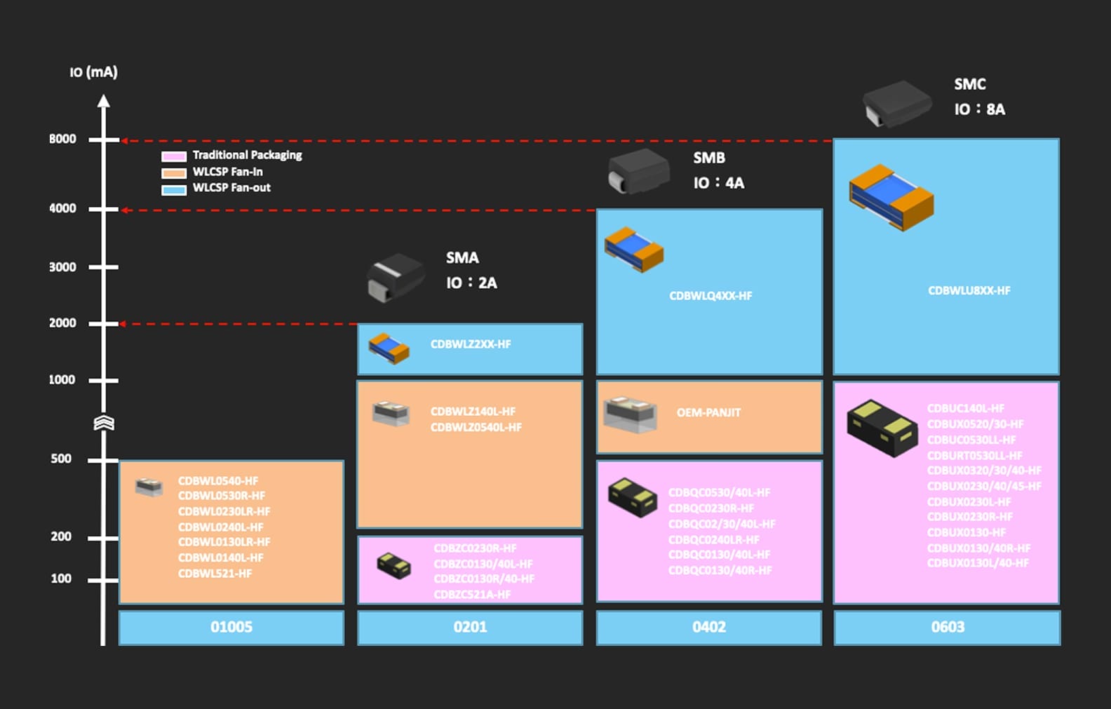
CSP VS WLCSP : Wafer Level Chip Scale Package
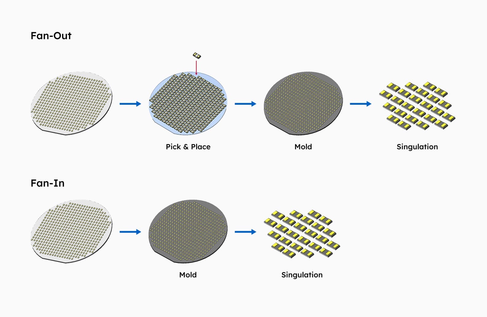
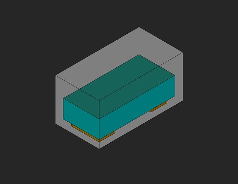
WLCSP : Die size / Package size = 90 – 100 %
Mold Type : Die size / Package size = 20 – 30 %
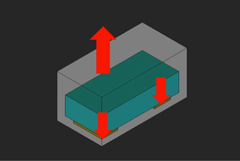
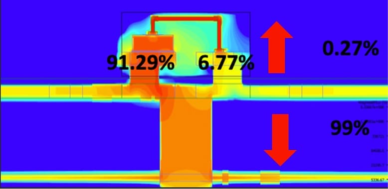
There are three main paths for transferring heat:
1. The heat source on the chip surface is transferred to the component surface through the mold compound by convection and radiation.
2. The heat is transferred from the chip surface through the bonding wire and then from the bonding pad to the PCB board for convection and radiation.
3. From the chip surface to the crystal seat, and then transferred from the PCB board by the solder pad for convection and radiation.
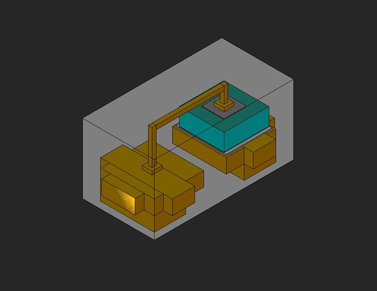
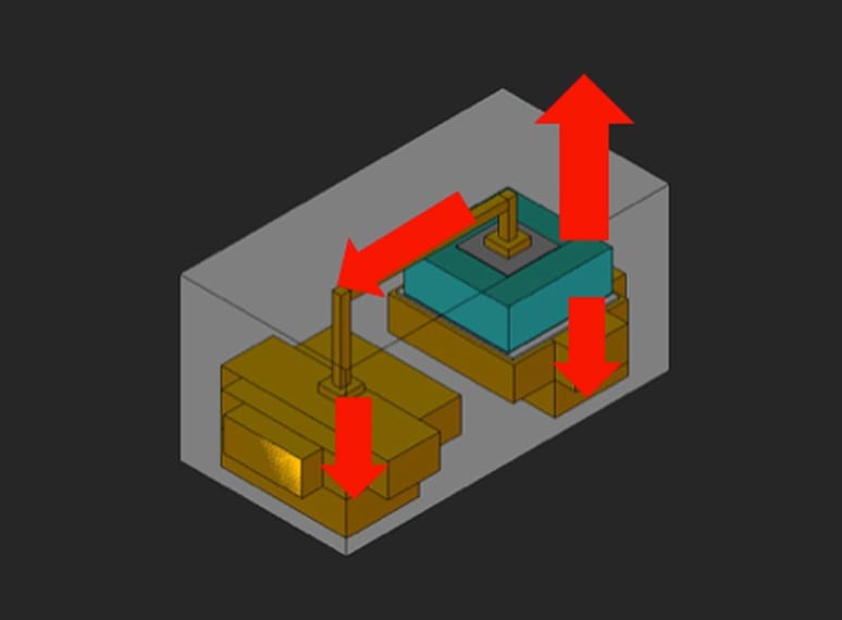
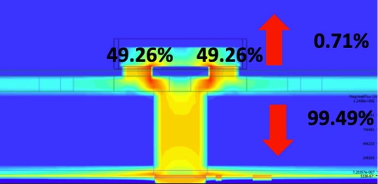
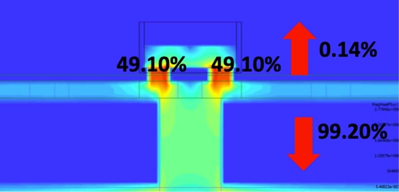
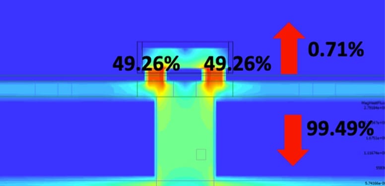
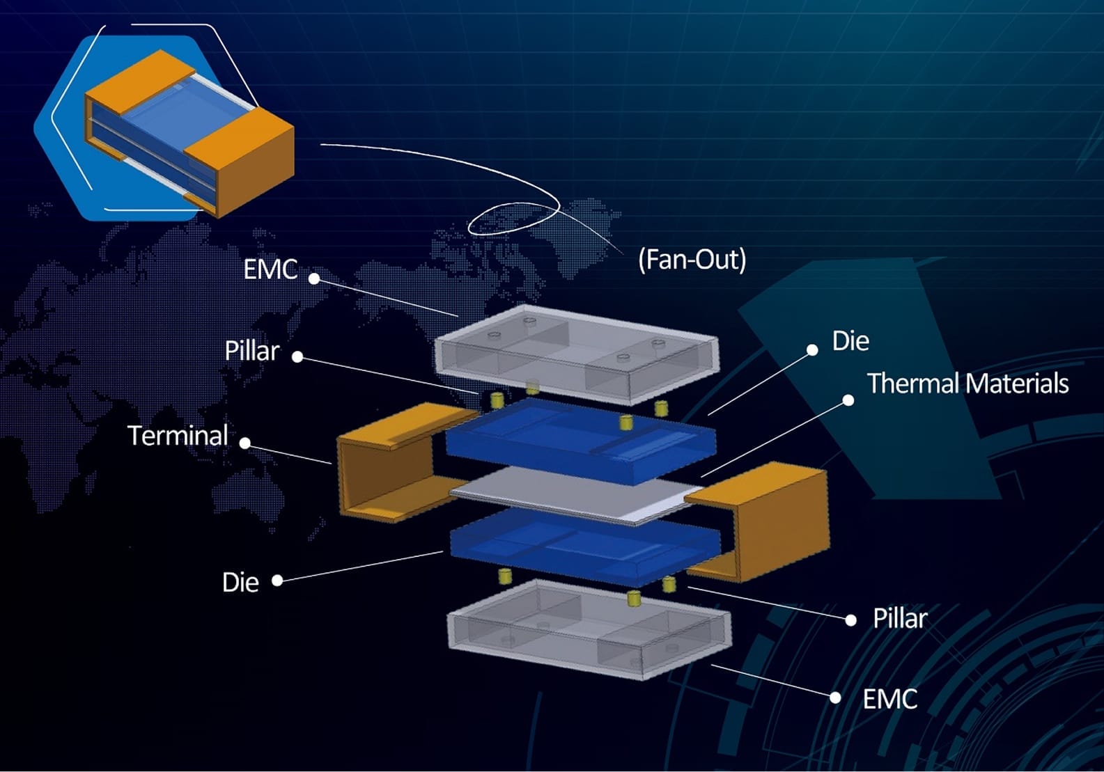
There are two main paths for transferring heat:
1. The heat source on the chip surface is transferred to the component surface through the mold compound by convection and radiation.
2. The heat is transferred from the chip surface through the copper pilar and then from the solder pad to the PCB board for convection and radiation.
<0201 Mold Type> 𝜃JA = 227.6 K/W ; 𝜃JB = 123.76 K/W ; 𝜃JC = 122.91 K/W
<0201 WLCSP> 𝜃JA = 135.48 K/W ; 𝜃JB = 31.81 K/W ; 𝜃JC = 65.53 K/W ; Mold R𝜃J / WLCSP R𝜃J = 45 - 65% ; Mold TJMax < WLCSP TJMaX
<01005 WLCSP (0.2mm)> 𝜃JA = 165.68 K/W ; 𝜃JB = 64.88 K/W ; 𝜃JC = 118.27 K/W
<01005 WLCSP (0.15mm)> 𝜃JA = 165.69 K/W ; 𝜃JB = 63.82 K/W ; 𝜃JC = 77.61 K/W ; Thick R𝜃J > Thin R𝜃J ; Thick TJMax ≈ Thin TJMax
Schottky : I/O = 100mA VF=0.538V
𝜃JA is the thermal resistance from the die surface to the surrounding environment
𝜃JB is the thermal resistance from the die surface to the circuit board
𝜃JC is the thermal resistance from the die surface to the package case
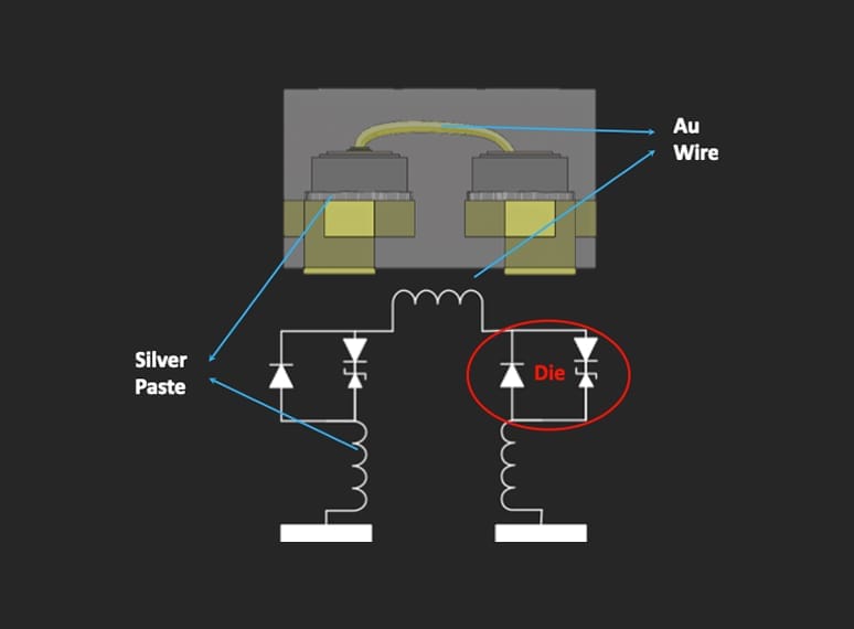
Parasitic element:
Die to Die → Au Wire
Die to Substrate → Silver Paste
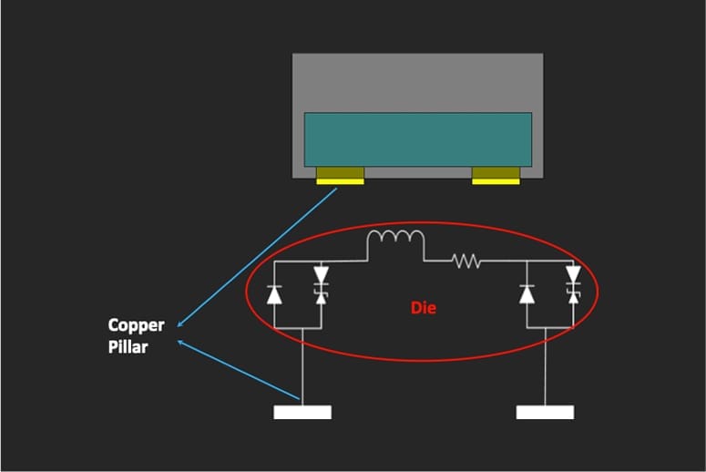
Parasitic element:
No Wire
No Substrate
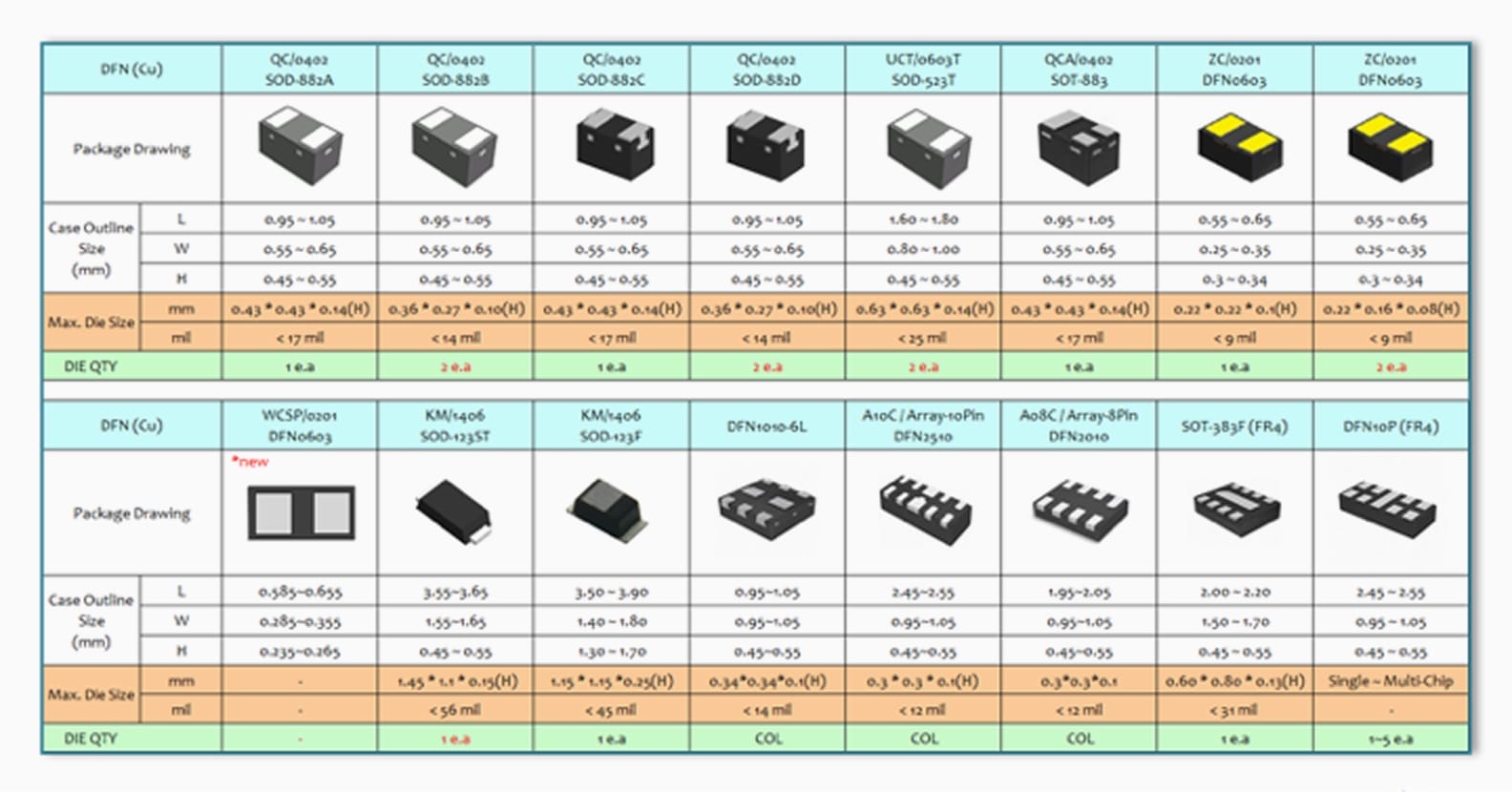
DFN products are manufactured in Comchip Taiwan’s manufacturing factility.

Comchip's 0402, 0603, and 1005 packages include a special side-wettable flank design for enhanced solderability.
Welcome to the “COMCHIP Technology Website” (hereinafter referred to as "this
Website").
To ensure that you can use the services and information provided by this Website with
peace
of mind, we hereby explain our Privacy Policy to protect your rights and interests. Please read the
following carefully: