


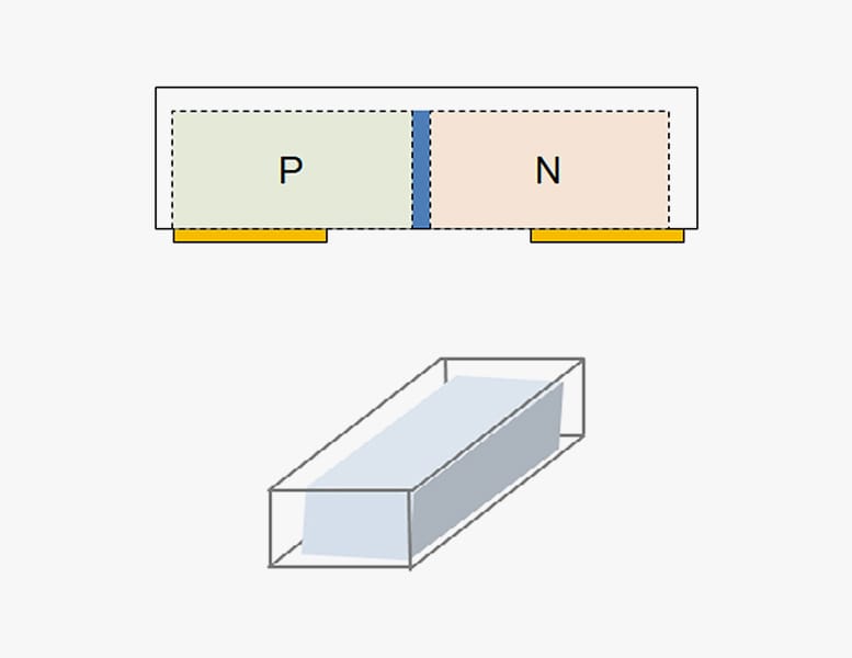
Chip-to-package ratio in wire bonding process
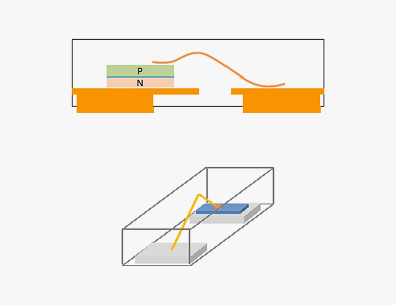
Chip-to-package ratio in WLCSP process
Comchip leads the industry with WLCSP diode packaging technology for ultra-compact electronic devices.
Chip-to-package ratio in wire bonding process
Chip-to-package ratio in WLCSP process
With the evolution of product applications and manufacturing processes, traditional diode packaging methods such as wire bonding and soldering are gradually falling short of meeting the needs of new-generation products. Particularly in handheld electronic devices, where designs are becoming increasingly compact and slim, along with growing demands for battery efficiency, PCB space is constantly shrinking—directly impacting component selection. Beyond improving performance, today's components must also meet stringent size requirements that continually challenge the limits of manufacturing and product design.
Comchip has long been a leader in the development of ultra-small package components and is now at the forefront of process innovation. The company has introduced a six-sided molded WLCSP ESD protection diode, setting a new industry benchmark with the launch of the smallest 01005 (0.4 x 0.2 mm) package. The process is also upward-compatible, supporting 0201 (0.6 x 0.3 mm) and paving the way for the development of various diode types using WLCSP technology, showcasing its advantages across a broader product range.
Traditional diode production uses a vertical P/N chip structure, requiring packaging methods like wire bonding or soldering to align the anode and cathode on the same side. Due to frame limitations, the actual chip size in such packaging is typically less than one-tenth of the package size, restricting power output. WLCSP, however, eliminates these constraints by maximizing chip usage within the same package footprint—enabling compact components with improved power handling and functional performance for space-constrained applications.
NEXT
Welcome to the “COMCHIP Technology Website” (hereinafter referred to as "this
Website").
To ensure that you can use the services and information provided by this Website with
peace
of mind, we hereby explain our Privacy Policy to protect your rights and interests. Please read the
following carefully: